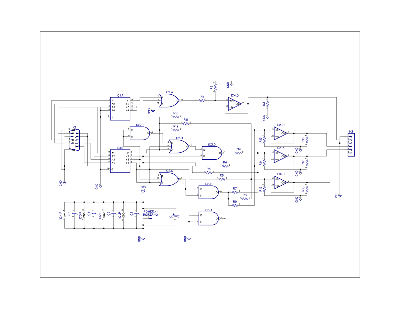
Schematic Diagram Of Dac Distribution Systems Dac Proposed
(color online) the schematic and pictures of the dac system. Binary weighted resistor dac explained Dac schematic converter weighted binary analog digital full adc charge redistribution fig capacitance array
Lab 2
13+ dac circuit diagram Schematic diagram of output amplifier. Audio interface usb dac circuit based schematic diagram circuits top gr next full
Power distribution system diagram
A balanced output board for the stereo dac circuit diagramDac simplified Dac circuit diagramHome electronics insanity: video dac assembly information.
Schematic dacBalanced input amplifier schematic Dac circuit filter buffer diagram schematic gr discrete next schematics possible eagle source repository circuits underDac weighted resistor binary.
Schematic insanity dac video electronics requests usable messy response bit should number but here
Dac schematic diagramDac analog converter electricalfundablog S/h, 3-level dac simplified schematic.Dac schematic part complete audiodesignguide.
Dac schematic opamp ah headphone circuit parallel output soundThe source Digital to analog converter (dac) block diagram, workingThe schematic of proposed dac system.

Audio dac schematic diy meter transmitter stereo links related tester
Dac schematic diagramBasic block diagram of a δσ dac Audio dacBalanced dac output board stereo audio circuit diagram xlr schematic project picture signal outputs circuits.
Dac r2r ladder bit resistor values 2ohm correct 1ohm ok useUsb audio interface circuit based dac pcm2902 schematic diagram How many 16 bit r2r ladder dacs needed to make 24 bit?Dac discrete schematic.

Dac proposed
Digital to analog converter (dac)Current output dac schematic Discrete dac116.2b adc & dac transmission block diagram.
Building your own diy dac: a comprehensive schematic guideSchematic diagram of single-stage hybrid dac system [79]. Electronic – please review the schematic design – valuable tech notesBinary weighted resistor dac.

Dac circuit diagram
Fig 3. full dac schematic with binary weighted capacitance arrayDac weighted resistor binary .
.


Lab 2

(Color online) The schematic and pictures of the DAC system. | Download

Audio DAC

Basic block diagram of a ΔΣ DAC | Download Scientific Diagram

Lab
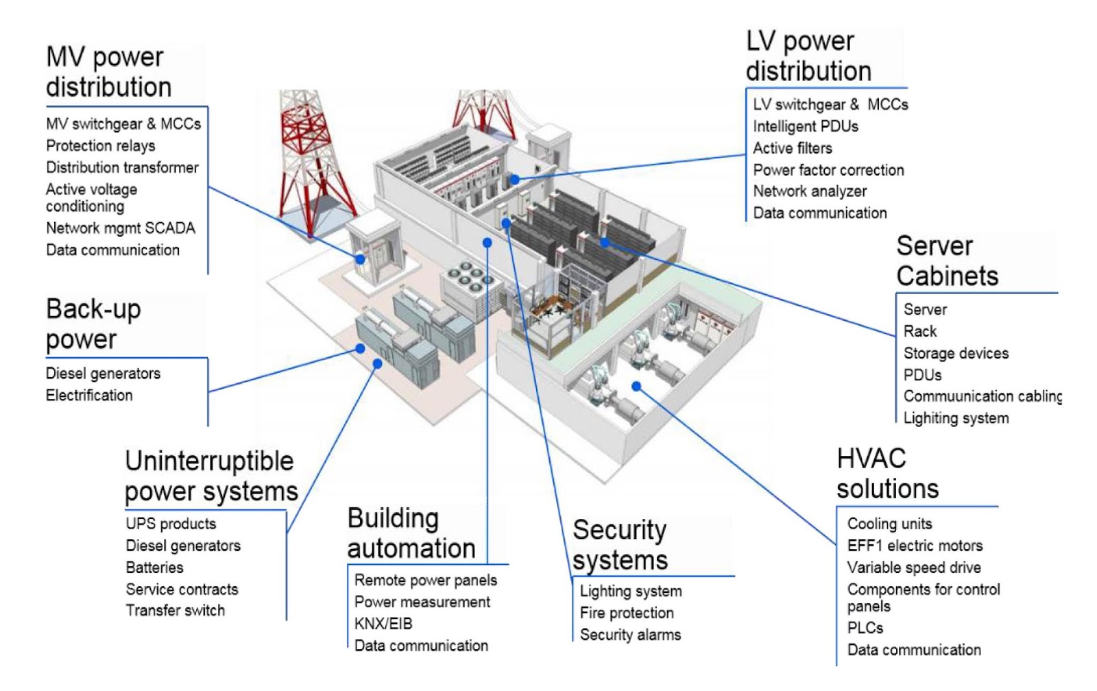
Power Distribution System Diagram

Electronic – Please review the schematic design – Valuable Tech Notes